


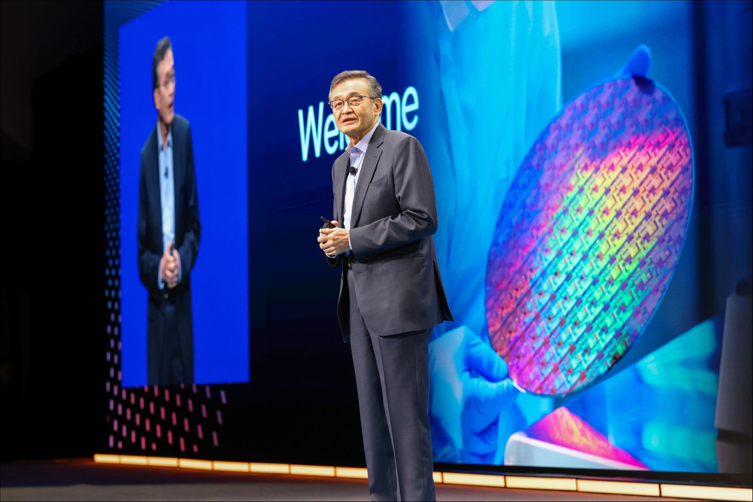
Intel CEO Lip-Bu Tan (Image Source: Intel)
AsianFin -- Following TSMC’s announcement of progress on its 1.8nm technology on April 24, Intel has revealed major updates to its Intel Foundry Services roadmap, signaling a deepening competition in next-generation semiconductor manufacturing.
Speaking at the 2025 Intel Foundry Conference in San Jose, California on April 29, Intel CEO Lip-Bu Tan announced that the company’s Intel 18A (1.8nm-class) process has officially entered the risk production phase. The Fab 52 facility in Arizona has already completed the tape-out for Intel 18A and is on track to begin full-scale mass production later this year.
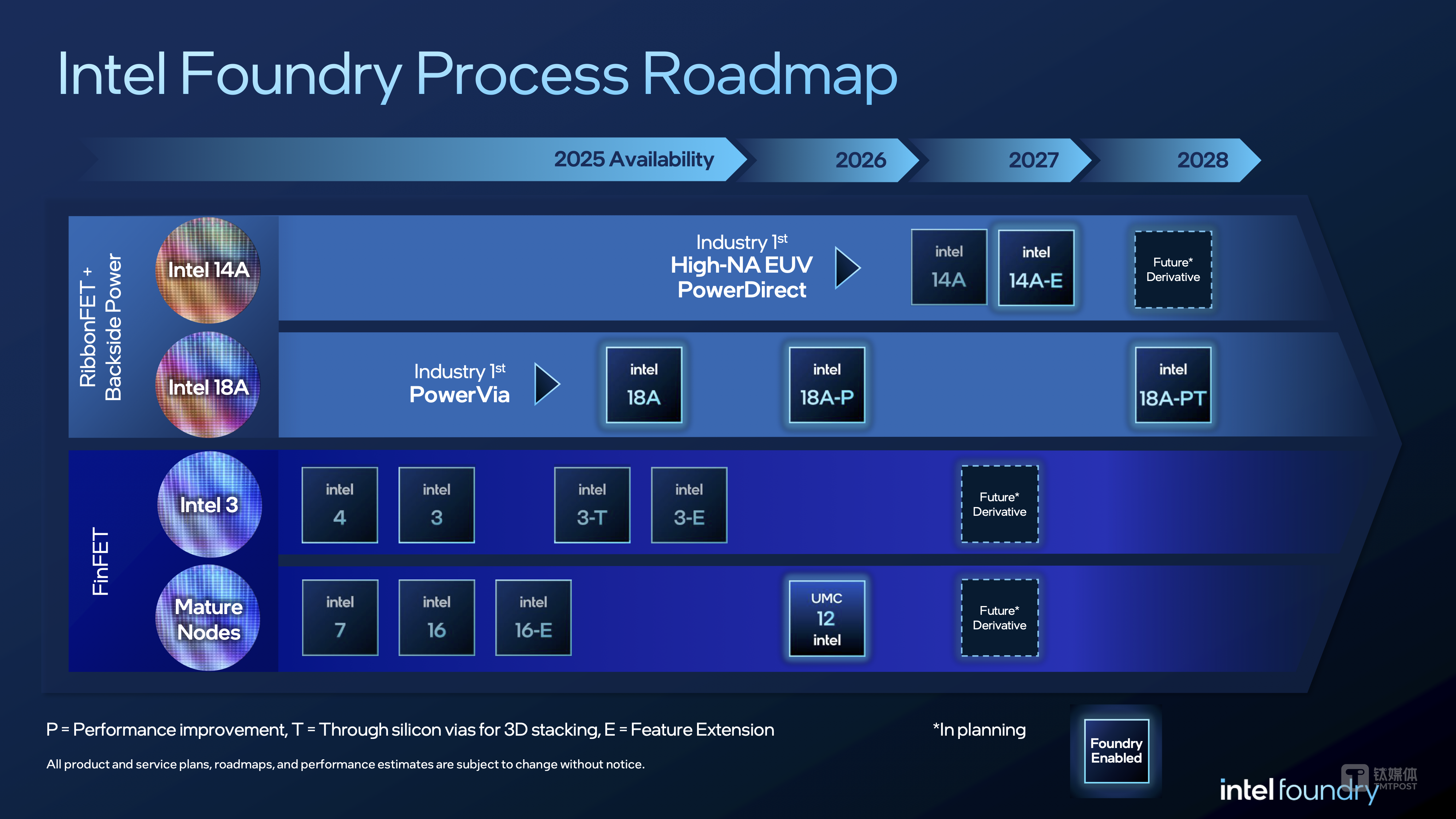
Intel also introduced several new process iterations, including Intel 18A-P, Intel 18A-PT, and its most advanced node to date—Intel 14A, a 1.4nm-class technology. The company expects these next-generation nodes to deliver a 15%–20% improvement in performance per watt over the standard 18A process. Intel aims to roll out products based on the 14A node around 2027.
“I will ensure the success of our foundry business.” Tan emphasized the importance of customer-centricity, pledging to listen to client feedback, enhance Intel’s product offerings, and partner closely with the U.S. government to build what he called a “great American foundry.”
His remarks follow mounting speculation that Intel might divest its foundry unit following recent leadership changes. Tan’s public statement serves as a direct rebuttal to those rumors and signals Intel’s long-term commitment to competing at the forefront of global semiconductor manufacturing.
Meanwhile, Taiwan Semiconductor Manufacturing Company (TSMC) continues to push its own technology roadmap. In April, the company confirmed that its 2nm (N2) process will enter mass production in the second half of 2025. TSMC also revealed that its 1.4nm-class A14 process is scheduled for mass production by 2028, with an enhanced A14 SPR version to follow in 2029.
These timelines set up a new flashpoint in the race between Intel and TSMC, with 2028 expected to mark a pivotal moment in the battle for 1.8nm supremacy. Both firms are vying to outpace Samsung, which has struggled with yield issues in its advanced process nodes.
While the world’s leading chipmakers push forward on bleeding-edge technology, China’s major foundries such as SMIC and Huahong remain focused on mature nodes—primarily 28nm and above. Only a handful of their lines currently produce 16/12nm chips. IDC forecasts that China’s mature-node chip production will account for 28% of global capacity by 2025, while SEMI predicts that share could rise to 39% by 2027.
This raises a strategic question: should China pursue advanced process technology like TSMC and Intel?
According to Professor Wei Shaojun of Tsinghua University, who chairs the Integrated Circuit Design Branch of the China Semiconductor Industry Association, the answer lies in pivoting away from conventional paths. He argues that with external constraints limiting access to advanced manufacturing equipment and IP, Chinese firms should shift focus toward design-driven innovation—leveraging architecture and microsystem integration rather than chasing smaller nodes. “The key is to break path dependency and establish a technological framework with Chinese characteristics,” Wei said.
The financial burden of chip innovation is also becoming unsustainable. Handel Jones, CEO of International Business Strategies (IBS), estimates the average design cost for a 28nm chip is around $40 million. That figure balloons to $217 million at 7nm, $416 million at 5nm, and $590 million at 3nm. All-in development costs for a 3nm chip can approach $1 billion, driven by expensive wafer runs, EUV lithography equipment, and low initial yields.
Looking ahead, the cost to develop a 2nm chip could exceed $725 million, potentially surpassing even 3nm due to higher R&D, equipment, and process complexity.
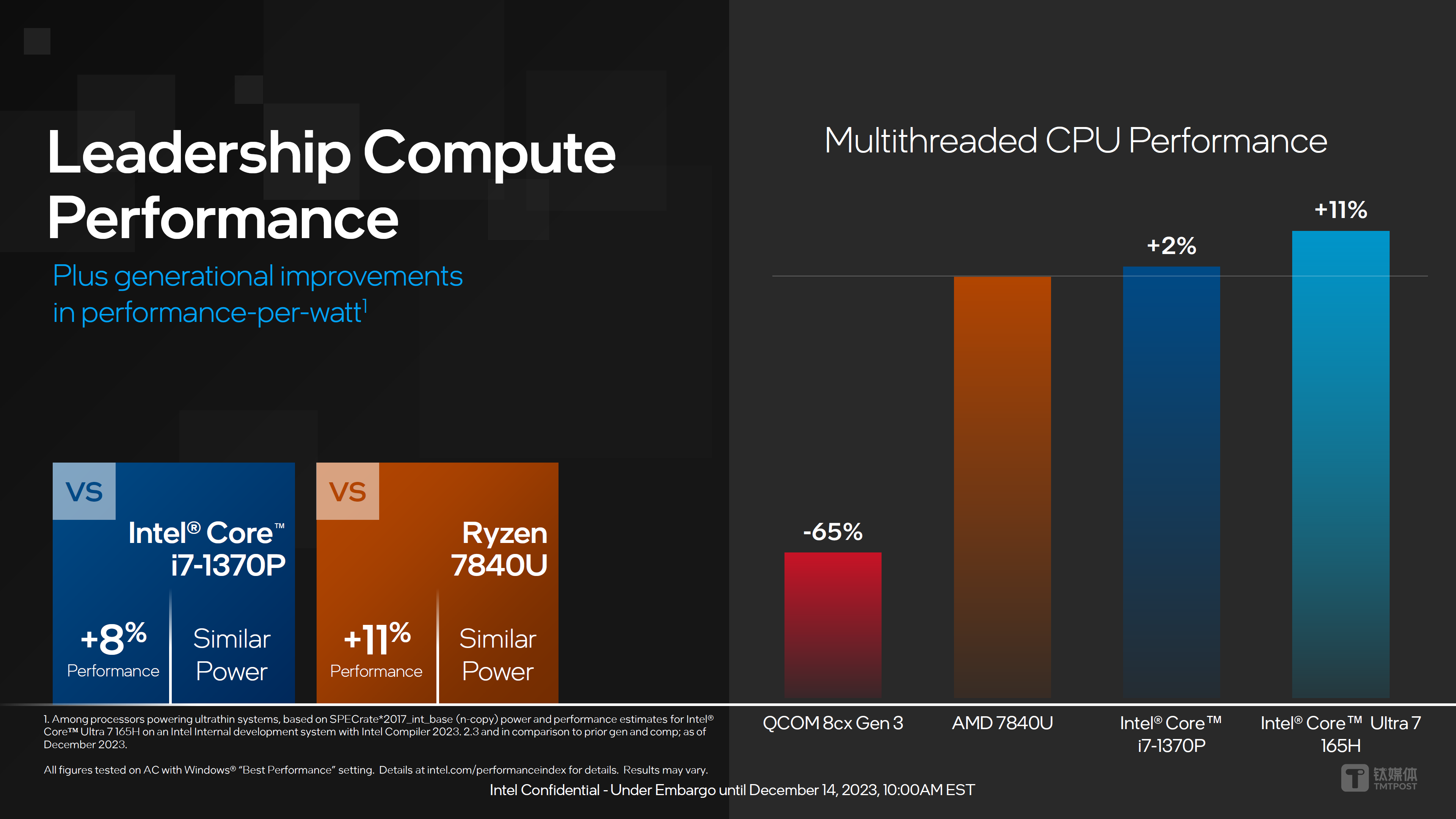
Despite these rising costs, the return on performance, power efficiency, and chip area (PPA) is slowing. For example, Qualcomm’s Snapdragon 8s Gen 4, built on a 4nm node, delivers a 31% CPU boost and 49% GPU performance increase—with energy efficiency up 39%. Intel’s Core Ultra 7 165H, built on its newest process with chiplet integration, offers just an 8% improvement in performance per watt over the previous 10nm Core i7-1370P.
Despite the enormous investments required to push chip manufacturing to more advanced nodes, the performance gains—particularly in CPU capabilities—have been increasingly underwhelming. Industry observers note that the cost-performance tradeoff has become harder to justify. This trend is underscored by NVIDIA CEO Jensen Huang, who is now placing greater emphasis on the surging demand for AI model tokens and the strategic role of the company’s latest B200 chip in the evolving AI landscape.
A semiconductor insider told TMTPost that domestic Chinese chipmakers are right to avoid chasing leading-edge process technologies. “Beyond 12nm, the impact of further process shrinking on overall performance becomes marginal,” the person said, adding that innovation should instead focus on design, system integration, and architecture.
Still, as the global chip race pushes toward the 1.8nm era, both Intel and TSMC are pursuing new breakthroughs aimed at achieving meaningful improvements in PPA—power efficiency, performance, and area.
Intel, for its part, has taken a bold step by scrapping plans for mass production of its 20A node and moving directly to Intel 18A, equivalent to 1.8nm. Intel 18A is the first process node in the industry to combine PowerVia—its backside power delivery network (BSPDN)—with RibbonFET, a next-generation gate-all-around (GAA) transistor architecture.
PowerVia relocates power delivery to the backside of the chip, enhancing performance and enabling higher transistor density. Intel claims this boosts ISO power efficiency by 4% and increases standard cell utilization by 5% to 10%. RibbonFET, meanwhile, uses four vertically stacked nanosheets fully surrounded by gates, delivering faster switching speeds and greater density in a smaller footprint.
Intel’s 18A process node has now entered the risk production phase. The company’s Fab 52 plant in Arizona has successfully completed Intel 18A tape-out, with initial small-batch production already underway. Mass production is scheduled to begin by the end of the year.
Intel revealed that the 18A node is expected to enter volume production in the second half of 2025 to support the launch of its first Panther Lake SKU by year-end, with additional SKUs to follow in the first half of 2026.
According to analysis from Tom’s Hardware, while TSMC still holds an advantage in transistor density—and possibly cost—Intel’s node offers faster performance and lower power consumption. However, the practical benefits may vary depending on specific chip designs.
Intel’s next-generation node after 18A is 14A, which is currently in development and planned for risk production in 2027.
If all goes well, 14A will be the industry’s first node to adopt high numerical aperture extreme ultraviolet (High-NA EUV) lithography, whereas TSMC’s A14 (1.4nm) node does not utilize High-NA EUV.
Specifically, Intel’s 14A will feature the second generation of its PowerVia backside power delivery technology. The new PowerDirect scheme is a more advanced and complex approach, delivering power directly to each transistor’s source and drain via dedicated contacts. This minimizes resistance and improves power efficiency. Compared to the current PowerVia solution, PowerDirect offers more direct and efficient connections. Intel has already shared an early version of its Process Design Kit (PDK) for the 14A node with major customers. The PDK includes data, documentation, and design rules needed for chip design and validation.
Intel disclosed that the 14A node will deliver a 1.3x increase in transistor density over 18A. Performance-per-watt is expected to improve by 15%–20%, while power consumption at the same performance level could be reduced by 25%–35%. Several customers have already expressed interest in using the Intel 14A process for chip production.
In addition, Intel’s foundry ecosystem partners—including Synopsys, Cadence, and Siemens EDA—have provided EDA support, reference flows, and IP licensing for Intel 18A, enabling customers to start product design on this node.
By contrast, TSMC’s N2 (2nm) node does not feature backside power delivery. However, its upcoming A16 node will adopt a direct-contact backside power delivery network called Super Power Rail (SPR). A16 is essentially a derivative of the N2P node with SPR technology and is expected to enter production by the end of 2026.
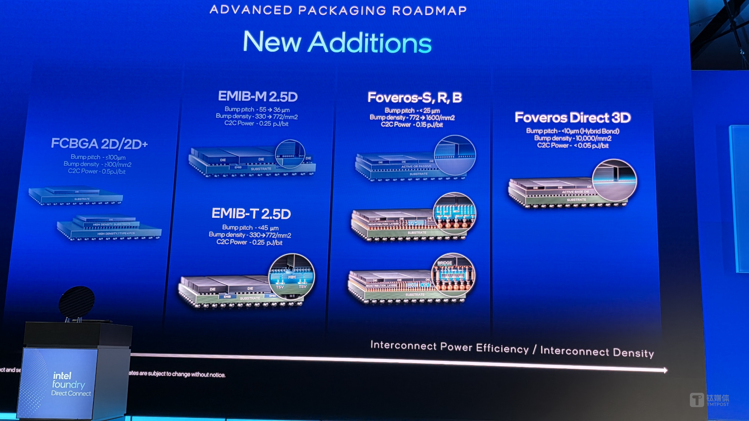
At a recent North America technology symposium, TSMC introduced a range of new innovations in logic processes, specialty processes, advanced packaging, and 3D chip stacking technologies.
SoW-X enables wafer-scale systems integrating at least 16 large compute dies, memory chips, fast optical interconnects, and new technologies on a single substrate. This provides kilowatts of power and up to 40 times the compute performance of current CoWoS solutions. TSMC also showcased its Compact Universal Photonic Engine (COUPE) for silicon photonics integration, N12 and N3 logic substrates for HBM4, and a new Integrated Voltage Regulator (IVR) solution for AI chips, which achieves five times the vertical power density compared to traditional discrete power management chips on circuit boards.
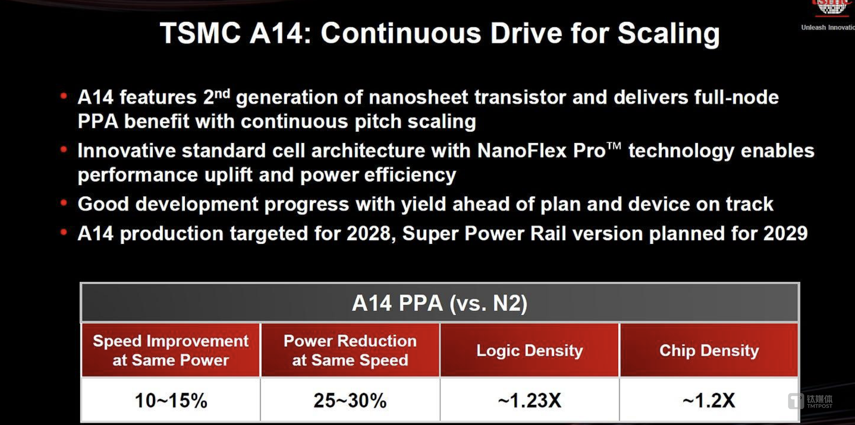
TSMC’s new A14 process will use second-generation GAAFET nanosheet transistors and upgrade its NanoFlex standard cell architecture to NanoFlex Pro with design-technology co-optimization (DTCO) for better performance, energy efficiency, and design flexibility.
Compared to N2, A14 will offer a 15% speed increase at the same power level or a 30% reduction in power at the same speed, along with a logic density improvement of over 20%. It is scheduled to go into production in 2028, with the initial version not featuring backside power delivery.
As demand for high-performance AI chips continues to surge, Nvidia—one of TSMC’s major clients—is pushing the envelope with its chiplet strategy. While its current flagship GPU uses a dual-chiplet design, the upcoming Rubin Ultra, expected in 2027, will feature four AI chips, all manufactured by TSMC.
TSMC remains firmly on track with its advanced process node roadmap. The chipmaker is expected to begin mass production of 2nm chips for clients like Apple and Nvidia later this year. Meanwhile, Intel is positioning itself as an aggressive reformer under Tan, who has implemented workforce restructuring and accelerated the company's transition to next-generation manufacturing nodes. Gelsinger is also focused on improving customer efficiency and winning back key accounts for Intel's contract manufacturing business.
Intel Foundry posted $4.7 billion in revenue in the first quarter of 2025, up 7% from a year earlier, according to the company’s latest earnings report.
“Our top priority is to manufacture Panther Lake for Intel’s internal customers,” Tan said, outlining the company’s foundry strategy. “The next step is to build trust with external clients and ensure we are executing reliably.”
In a company-wide letter this April, Tan described the current phase as a “make-or-break moment” for Intel. Flattening the executive team structure was just the beginning, he said, adding that the company must become more streamlined, efficient, and collaborative. “Intel was once considered the most innovative company in the world. If we push forward the necessary changes, there’s no reason we can’t return to the top,” he wrote.
“I know there is tremendous pressure. But we are behind, and we need to be united to fight for every win,” Tan added.
Intel’s 18A and 14A process nodes are progressing steadily, with plans to introduce a new 18A-PT variant designed for chip stacking. This move is expected to enhance Intel’s appeal to prospective foundry customers. However, no new details have been shared about the company’s roadmap for the Intel 3 or 10A (1nm) nodes, which are not expected to begin development until 2027.
Globalization of Chip Manufacturing Falters as TSMC, Intel Pour Billions into U.S. Expansion
The era of globally distributed chip manufacturing is showing signs of retreat, with industry giants like TSMC and Intel prioritizing local capacity building—especially in the United States.
TSMC has already committed over $200 billion to investments in the U.S., highlighting the growing importance of domestic chip production amid rising geopolitical and supply chain concerns.
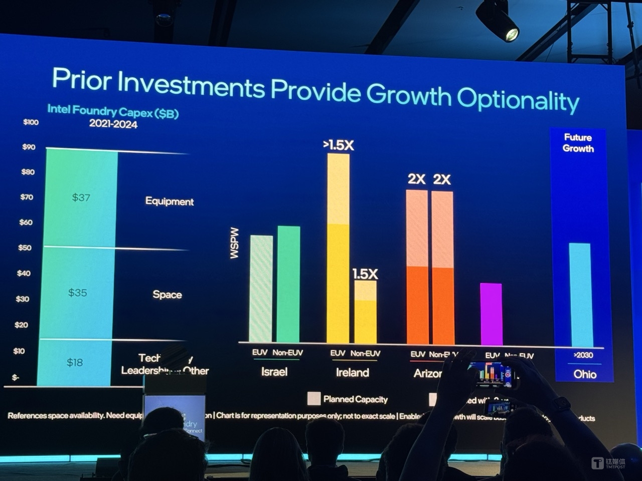
Intel, for its part, has made global foundry expansion a top strategic priority. According to the company, it invested nearly $90 billion in capital expenditures between 2021 and 2024. Of that, roughly 20% went toward enhancing front-end and back-end technological capabilities, while the remaining 80%—around $72 billion—was dedicated to increasing global manufacturing capacity. This includes investments in new equipment and the construction of advanced chip fabs around the world.
TSMC founder Morris Chang once declared that "globalization of semiconductors is dead" in the context of the U.S.-China chip war. He emphasized that free trade in semiconductors—particularly in cutting-edge chips—no longer exists.
In the wake of the global chip shortage crisis that erupted over the past two years, combined with rising deglobalization trends, both TSMC and Intel have ramped up efforts to establish new semiconductor manufacturing facilities aimed at enabling local production for local consumption.
In March this year, TSMC announced it would expand its U.S. investment to $165 billion—an increase of $100 billion. The plan includes the construction of three new chip fabrication plants, two advanced packaging facilities, and a major R&D center. The company estimates the expansion will generate 40,000 construction jobs and tens of thousands of high-paying roles in chip manufacturing and research. Over the next decade, the project is expected to contribute more than $200 billion in indirect economic output in the U.S.
U.S. President Donald Trump noted that TSMC's investment in the U.S. has now reached $200 billion, calling it one of several major technology investments during his potential second term. According to projections from the U.S. Department of Commerce, the country could be producing around 20% of the world's advanced chips by 2030—up from virtually none today.
Intel, however, has faced greater challenges. Construction of its planned chip factories in Poland and Germany has been delayed. On June 19, 2023, Intel signed a revised investment agreement with the German federal government to build two state-of-the-art fabs in Magdeburg, Saxony-Anhalt, investing more than €30 billion, with production of sub-1.8nm chips targeted for 2027. The German government committed €10 billion in subsidies.
Yet by September 2024, Intel announced a broad cost-cutting initiative, including a two-year delay to its Fab 29 construction in Magdeburg. Recently, the company even began restoring the purchased land back to agricultural use.
TSMC’s Arizona plant has also been costly. In its annual report, the company revealed operating losses of NT$4.81 billion, NT$9.43 billion, and NT$10.924 billion in 2021, 2022, and 2023, respectively. Before mass production begins in Q4 2024, cumulative losses over the past four years at this site have already surpassed NT$39.4 billion, making it TSMC’s most expensive overseas facility.
According to McKinsey, even when accounting for subsidies, building a standard mature-node logic fab in the U.S. costs about 10% more than in Asia. Operating costs are up to 35% higher. While Europe offers lower labor costs, its higher energy prices put operating expenses on par with those in the U.S.
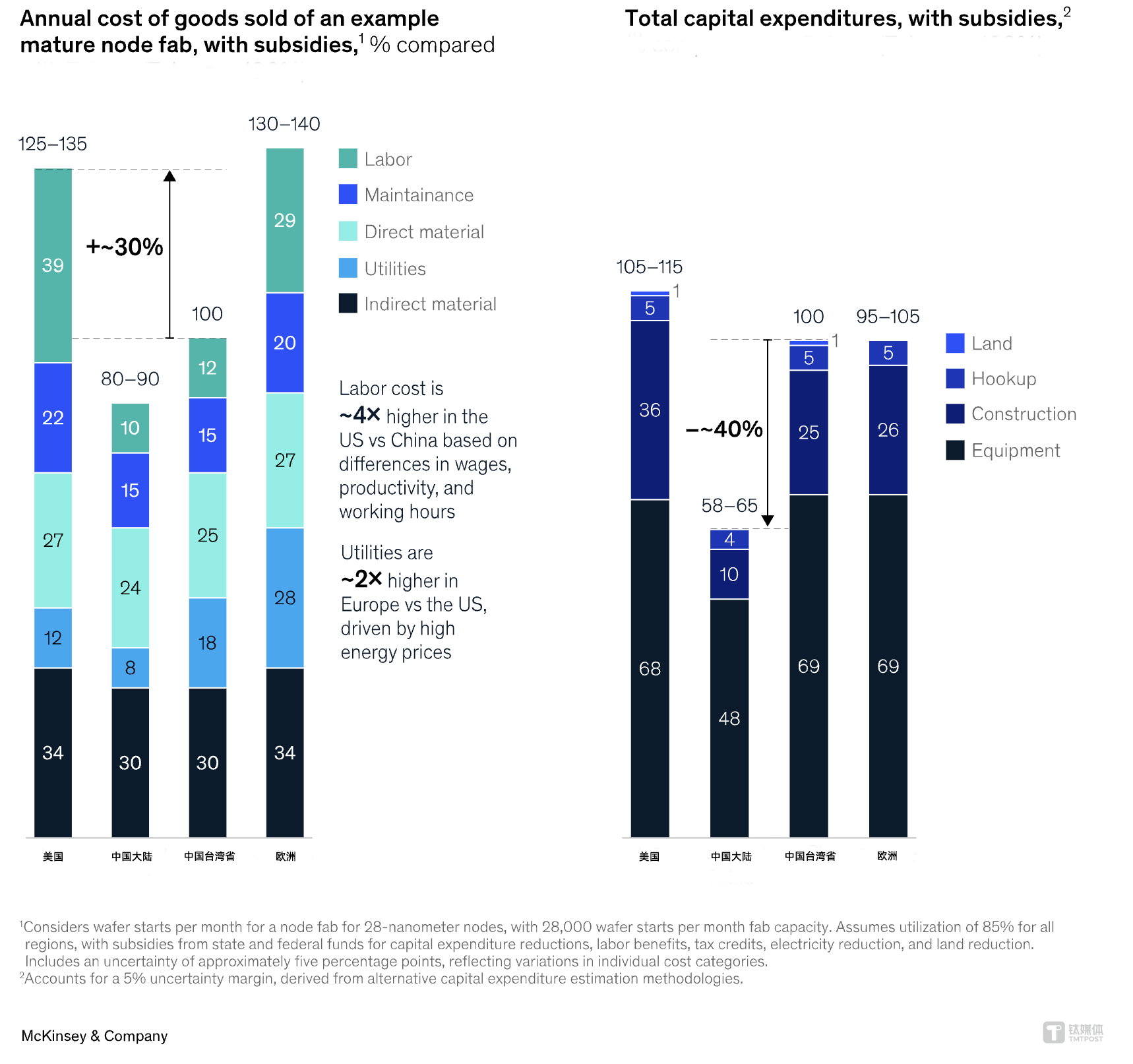
According to McKinsey, five key factors are driving the rising costs of building and operating semiconductor fabs in the U.S.: fundamental capital and operational cost dynamics, surging material demand, overseas concentration of raw materials and packaging, logistics and handling challenges, and a persistent talent shortage.
Among these, labor costs stand out as a major contributor. Direct labor accounts for around 30% of a U.S. fab’s total operating expenses, while maintenance represents 20%. U.S. labor costs are two to four times higher than in Asia. Given that chip manufacturing relies heavily on maintaining utilization rates above 75% to be economically viable, this poses a significant burden.
Data from Semiconductor Intelligence shows that global semiconductor capital expenditure is expected to fall 5% in 2024 to $155 billion, down from $168 billion in 2023. However, spending is projected to rebound by 3% in 2025, reaching $160 billion, largely driven by increased investments from TSMC and Micron.
TSMC’s capital spending is forecast to grow more than 30% in 2025 to between $38 billion and $42 billion, with AI-related revenue expected to double. Micron, meanwhile, projects a 73% year-over-year increase in capital expenditure for its fiscal year ending August 2025, reaching $14 billion. Excluding TSMC and Micron, global semiconductor capex in 2025 would decline by $12 billion—or 10%—from 2024 levels.
At the recent SEMICON China trade show, industry group SEMI projected that global semiconductor equipment investment would reach $121.5 billion in 2025, rising further to $139.4 billion in 2026. Between now and 2027, 105 new fabs are expected to come online, 75 of which will be located in Asia. By then, global wafer fab equipment (WFE) spending could exceed ¥1.22 trillion (approx. $170 billion).
Commenting on the geopolitical divide in the chip sector, Wei Shaojun, a prominent semiconductor industry expert in China, remarked, “The idea of a world split into two tech ecosystems led separately by the U.S. and China may sound plausible, but from an industry development perspective, such an outcome would be a tragedy—potentially a lose-lose scenario for all.” He emphasized that despite the shifting global landscape, China’s semiconductor industry must remain confident and focused on long-term growth.
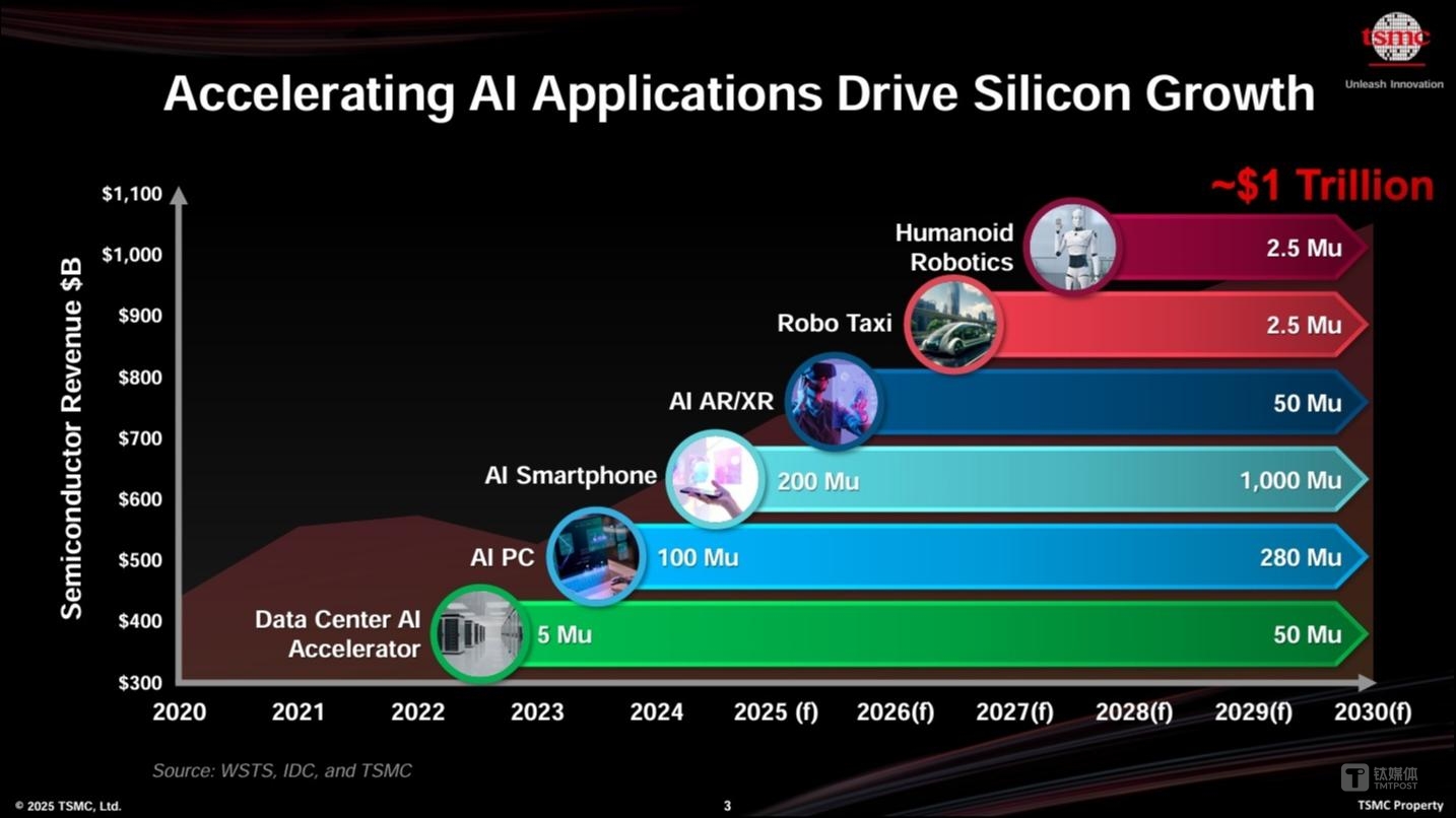
Zhang Xiaoqiang, TSMC Senior Vice President of Business Development, said the rapid advancement of AI could push global semiconductor industry revenue beyond the $1 trillion mark before 2030. He noted growing demand for AI data servers and AI-enabled smartphones, while cautioning that investors should remain vigilant in light of recent U.S. tariff hikes and concerns over a potential AI bubble.
Looking ahead to 2025, the World Semiconductor Trade Statistics (WSTS) forecasts the global semiconductor market will grow by 11.2% year-over-year to $697 billion. Industry group SEMI anticipates that AI will drive an 18% increase in global semiconductor manufacturing investments by 2026, supporting industry expansion to $1 trillion by 2030 and surpassing $2.1 trillion by 2035.
According to McKinsey, semiconductor companies worldwide are expected to invest around $1 trillion in new wafer fabrication facilities by 2030 to meet soaring demand driven by AI and digital transformation.